


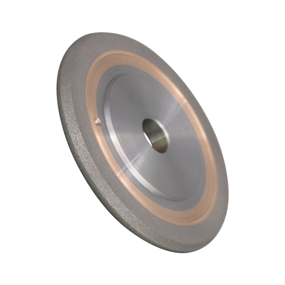
Resin bond diamond dicing blades(soft blades) has good elasticity, self-sharpening, sharp cutting, good cutting quality
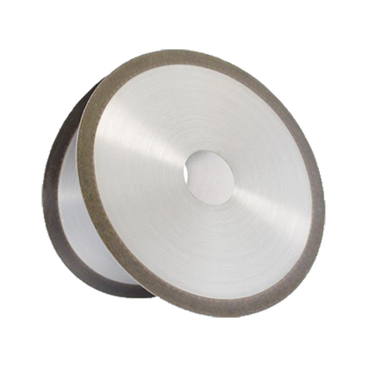
Metal bond diamond dicing blades (soft blades) have high strength, good rigidity, long life
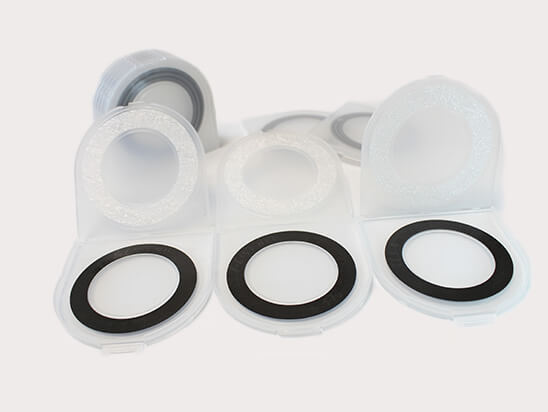
Electroplated bond diamond dicing blades (soft blades) feature high strength, good rigidity, good shape retention and long service life.
|
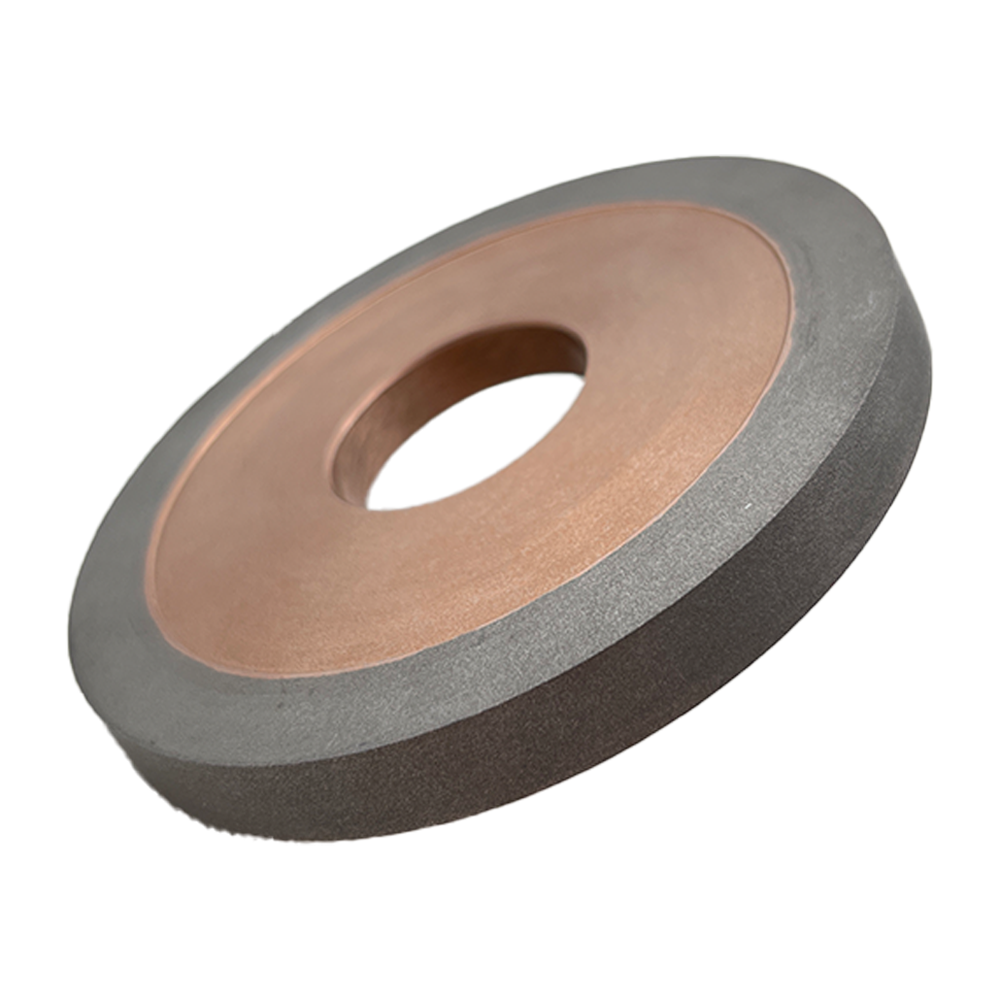
1.Metal bond dicing balde
Application: Scribing electronic parts, optical devices, semiconductor packages, BGA, CSP, PCB, ceramic, glass, quartz, crystal, ferrite, optical communication (Faraday), etc
2.Resin bond dicing blade
Application: cutting scribing glass (optical devices, fiber optics), quartz (optical splitters, saw devices), LiTa03 LiNb03 (devices), BGA, QFN (copper epoxy molding ), splitter, sapphire, ceramic substrate, alumina, aliminum nitride, etc
3.Electroformed dicing balde
Application: Scribing dicing silicon wafers, copper wafer and compound semiconductor wafers ( such as GaAs and SiC) , resistance, ceramic, packaging materials, lithium niobate, lithium tantalate, etc
-

12A1 Wafer hub dicing saw blade Diamond Dicing ...
-
Hybrid Bond Diamond Grinding Wheels For Broach ...
-

Resin Bond CBN Grinding Wheel Ski and Snowboard...
-
1A1R Ultra Thin Resin Bond Diamond Cutting Disc...
-

Internal Grinding Of Vitrified CBN Inner Wheel ...
-
14F1 Hybrid Bond Diamond Grinding Wheel For HSS...